INSUBCONTINENT EXCLUSIVE:
One way to do that is called remote epitaxy, where an intermediate layer made out of graphene or other material is introduced between the
substrate and the growing crystals
Once the epitaxy process is done, the substrate and everything on it are soaked in a chemical solution that dissolves this intermediate
layer, leaving the crystalline film intact
This works but is expensive, difficult to scale, and takes a lot of time
To make the process cheaper and faster, the MIT team had to grow the crystals directly on the substrate, without any intermediate layers
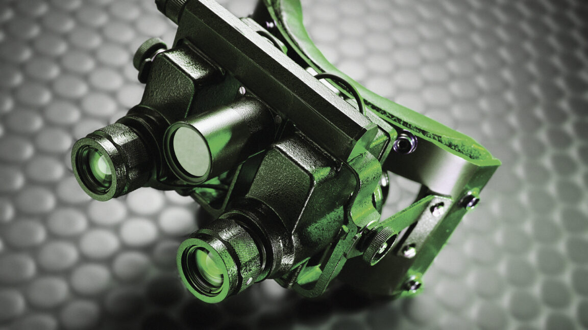
What they were trying to achieve was a non-stick frying pan effect but at an atomically small scale.The material that prevented the
When the team was experimenting with growing different films in their previous studies, they noticed that there was a material that easily
came off the substrate, yet retained an atomically smooth surface: PMN-PT, or lead magnesium niobate-lead titanate.The lead atoms in the
PMN-PT weakened the covalent bonds between the film and the substrate, preventing the electrons from jumping through the interface between
it had exceptional pyroelectric properties
Once the team realized they could manufacture and peel away PMN-PT films at will, they tried something a bit more complex: a cooling-free,
far-infrared radiation detector
of 10-nanometer-thin PMN-PT films, each about 60 square microns, that the team transferred onto a silicon chip
This produced a 100-pixel infrared sensor
Tests with ever smaller changes in temperature indicated that it outperformed state-of-the art night vision systems and was sensitive to
radiation across the entire infrared spectrum
(Mercury cadmium telluride detectors respond to a much narrower band of wavelengths.)